AAWSAP DIRD, Metallic Spintronics, March 2010
DOW-UAP-D129 · page 20 of 27
Text
This text came with the file. It may have mistakes. When the text and the image disagree, the image is right.
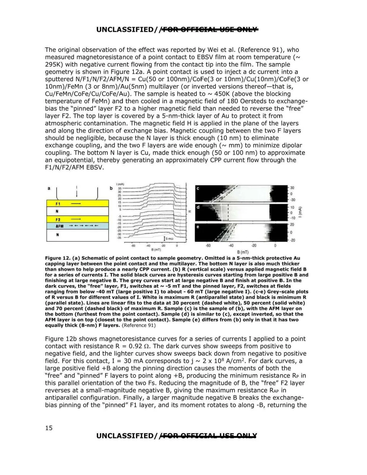
UNCLASSIFIED// FOR OFFIElIAk WSE OPtkY The original observation of the effect was reported by Wei et al. (Reference 91), who measured magnetoresistance of a point contact to EBSV film at room temperature ( ~ 295K) with negative current flowing from the contact tip into the film. The sample geometry is shown in Figure 12a. A point contact is used to inject a de current into a sputtered N/Fl/N/F2/AFM/N = Cu(50 or 100nm)/CoFe(3 or 10nm)/Cu(10nm)/CoFe(3 or l0nm)/FeMn (3 or 8nm)/Au(5nm) multilayer (or inv,erted versions thereof-that is, Cu/FeMn/CoFe/Cu/CoFe/Au). The sample is heated to ~450K (above the blocking temperature of FeMn) and then cooled in a magnetic field of 180 Oersteds to exchange bias the "pinned" layer F2 to a higher magnetic field than needed to reverse the "free" layer F2. The top layer is covered by a 5-nm-thick layer of Au to protect it from atmospheric contamination. The magnetic field H is applied in the plane of the layers and along the direction of exchange bias. Magnetic coupling between the two F layers should be negligible, because the N layer is thick enough (10 nm) to eliminate exchange coupling, and the two Flayers are wide enough ( ~ mm) to minimize dipolar coupling. The bottom N layer is Cu, made thick enough (50 or 100 nm) to approximate an equipotential, thereby generating an approximately CPP current flow through the Fl/N/F2/AFM EBSV. J F1 - N F2 - AFM - --- N "° 20 e , ,,,, , ·60 I I 0 ·20 0 30 0 .30 10 l 0 -10 - 20 0 ·20 B(mTJ B(mT) Figure 12. (a) Schematic of point contact to sample geometry. Omitted is a 5-nm-thick protective Au capping layer between the point contact and the multilayer. The bottom N layer is also much thicker than shown to help produce a nearly CPP current. (b) R (vertical scale) versus applied magnetic field B for a series of currents I. The solid black curves are hysteresis curves starting from large positive Band finishing at large negative B. The grey curves start at large negative B and finish at positive B. In the dark curves, the "free" layer, Fl, switches at ,.., -5 mT and the pinned layer, F2, switches at fields ranging from below -40 mT (large positive I) to about - 60 mT (large negative I). (c-e) Grey-scale plots of R versus B for different values of I. White is maximum R (antiparallel state) and black is minimum R (parallel state). Lines are linear fits to the data at 30 percent (dashed white), SO percent (solid white) and 70 percent (dashed black) of maximum R. Sample (c) is the sample of (b), with the AFM layer on the bottom (furthest from the point contact). Sample (d} Is similar to (c), except inverted, so that the AFM layer is on top (closest to the point contact). Sample (e) differs from (b) only in that it has two equally thick (8-nm) F layers. (Reference 91) Figure 12b shows magnetoresistance curves for a series of currents I applied to a point contact with resistance R = 0.92 n. The dark curves show sweeps from positive to negative field, and the lighter curves show sweeps back down from negative to positive field. For this contact, I = 30 mA corresponds to j ~2 x 10⁸ A/cm 2. For dark curves, a large positive field + B along the pinning direction causes the moments of both the "free" and "pinned" F layers to point along +B, producing the minimum resistance RP in this parallel orientation of the two Fs. Reducing the magnitude of B, the "free" F2 layer reverses at a small-magnitude negative B, giving the maximum resistance RAPin antiparallel configuration. Finally, a larger magnitude negative B breaks the exchange bias pinning of the "pinned" Fl layer, and its moment rotates to along -B, returning the UNCLASSIFIED/,' FOA OfifilCI0Lt !P&i Alf! Y 15