AAWSAP DIRD, Metallic Spintronics, March 2010
DOW-UAP-D129 · page 16 of 27
Text
This text came with the file. It may have mistakes. When the text and the image disagree, the image is right.
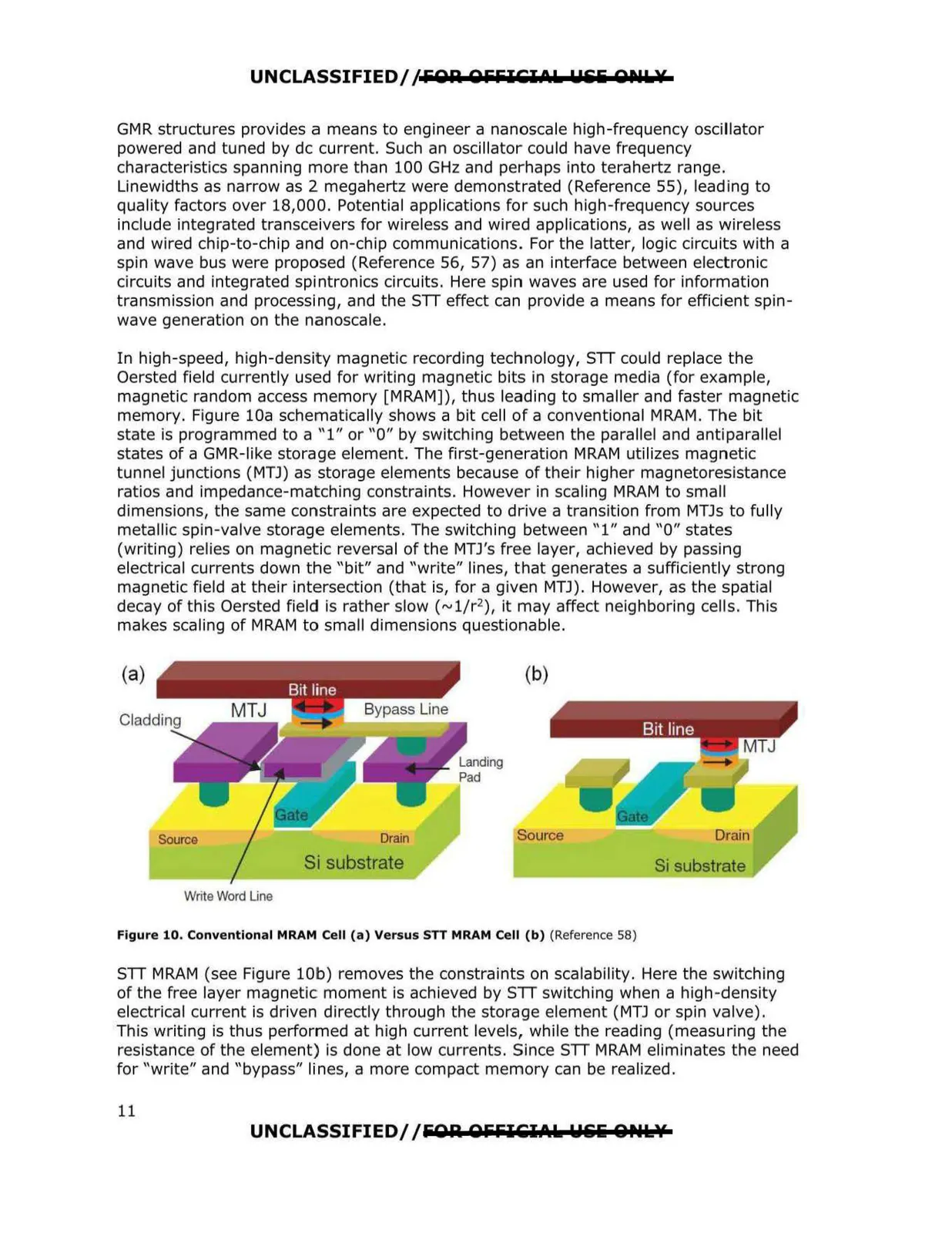
UNCLASSIFIED//FOA OFFIClal.k Wili 01\1k¥ GMR structures provides a means to engineer a nanoscale high-frequency oscillator powered and tuned by de current. Such an oscillator could have frequency characteristics spanning more than 100 GHz and perhaps into terahertz range. Linewidths as narrow as 2 megahertz were demonstrated (Reference 55), lead ing to quality factors over 18,000. Potential applications for such high-frequency sources include integrated transceivers for wireless and wired applications, as well as wireless and wired chip-to-chip and on-chip communications. For the latter, logic circuits with a spin wave bus were proposed (Reference 56, 57) as an interface between electronic circuits and integrated spintronics circuits. Here spin waves are used for information transmission and processing, and the STT effect can provide a means for efficient spin wave generation on the nanoscale. In high-speed, high-densit y magnetic recording technology, STT could replace the Oersted field currently used for writing magnetic bits in storage media (for example, magnetic random access memory [MRAM]), thus leading to smaller and faster magnetic memory. Figure 10a schematically shows a bit cell of a conventional MRAM. The bit state is programmed to a "1" or "0" by switching bet ween the parallel and antiparallel states of a GMR-like storage element. The first-generation MRAM utilizes magnetic tunnel junctions (MTJ) as storage elements because of their higher magnetoresistance ratios and impedance-matching constraints. However in scaling MRAM to small dimensions, the same constraints are expected to drive a transition from MTJs to fully metallic spin-valve storage elements. The switching between "1" and "O" states (writing) relies on magnetic reversal of the MTJ's free layer, achieved by passing electrical currents down the "bit" and "write" lines, that generates a sufficiently strong magnetic field at their intersection (that is, for a given MTJ). However, as the spatial decay of this Oersted field is rather slow (~1/r2), it may affect neighboring cells. This makes scaling of MRAM to small dimensions questionable. (b) (a) Source Drain Si substrate Write Word Line Si substrate Figure 10. Conventional MRAM Cell (a) Versus STT MRAM Cell (b) (Reference 58) STT MRAM (see Figure 10b) removes the constraints on scalability. Here the switching of the free layer magnetic moment is achieved by STT switching when a high-density electrical current is driven directly through the storage element (MTJ or spin valve). This writing is thus performed at high current levels, while the read ing (measuring the resistance of the element) is done at low currents. Since STT MRAM eliminates the need for "write" and "bypass" lines, a more compact memory can be realized. UNCLASSIFIED/ /FOR OFFICl.t.k Wili &NL¥ 11